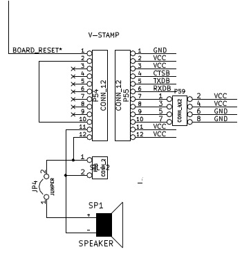
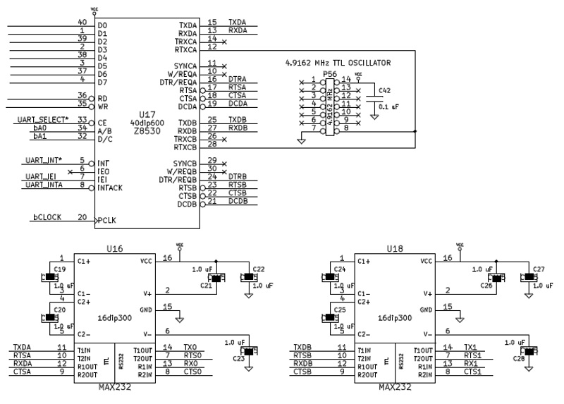
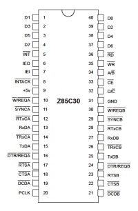
S100 Computers

Home S-100 Boards History New Boards Software Boards For Sale
Forum Other Web Sites Quiz Index    

A Serial IO S-100 Board
Introduction

Many S-100 systems have some kind of Serial IO board in their system.  Serial IO is primarily used for communication with a CRT terminal, though some printers also used serial IO.  With the advent of multi-user S-100 systems, serial IO was almost always used to connect the multiple terminals/users to the system. This was before the days of networking and the Internet!

The big advantage of serial IO over parallel ports for communications is the simplicity of the wired connection. Instead of 8 data lines, a strobe, an acknowledge line, serial communication can be as little as two lines, more often four and sometimes more.   The hardware however is more complicated since the data bits need to be sequentially sent along one wire.  Over the years numerous LSI chips were made to carry out this process. They are generally called UART's (Universal asynchronous receive/transmitter chips).  Commonly used chips in early S-100 systems were:-

General Instruments' AY-5-1013A. This was widely copied by SMC, TI, Western Digital and others later.   The chip however required a separate Baud rate generator (BRG, typically a 4702).

Next came the Intel 8251A type chips. These also could transmit in a "synchronous" data format where the transmitter and receiver shared a common clock signal. This was really never used in S-100 systems but the chip itself was commonly used. Again a separate Baud rate chip (4702) was required.

Signetics and National Semiconductor came up with the equivalent 2651 and 8250 chips.  These chips had the advantage of having the Baud rate generator onboard. It just requires a 5.068 crystal (2651) or the 2MHz S-100 bus signal (8250).

Motorola had its own 6800 type "ACIA" equivalent chip the MC6850. It is perhaps the easiest to configure but you need to "bend" the Intel style S-100 bus signals to use it. The TDL SMB was the most common case of its use on the S100 bus.

Not to be out done Zilog had their equivalent chip which they called the DART. It's big advantage was that it had two serial channels on one chip. It worked best is a Z80 hardware environment in an interrupt driven mode.

A number of S-100 Board manufactures started to add multiple chips to one board. A good example of this was the Cromemco TUART board which had two dual channel TMS 5501 UARTs on board.

One of the frustrating things about many of the earlier UART chips was the fact that internally they used a block if IO addresses for their many internal configuration registers.  A few of these chips on one board and bang, there goes a 20H address black.   In a  multi-card S-100 system finding a block of addresses that does not overlap with other cards can be a problem.

The Zilog Z85C30
SCC Pinout Enter the Zilog Z85C30 or SCC (Serial Communications Channel) chip as Zilog calls it.  This was Zilog's second generation UART type chip. Obviously it had the advantage testing of all previous chips but it evolved into an extremely powerful UART chip. It has the capability of doing almost any format of serial communications you could come up with. Some are quite exotic. It's a dual channel chip with its own internal BAUD rate generator, but best of all its easy to interface in terms of hardware.  Being a second generation chip it also has a large FIFO buffer to prevent data overruns.  As icing on the cake each channel requires only two IO ports to address its many internal registers.  The first port (address line = 0), address register 0 which is then loaded with the required register to be read or written to on the NEXT register read or write.  The second port (address line = 1) contains the I/O data.  This simple arrangement makes interfacing the chip a joy. Contrast this with a single channel 8250 which needs 3 address lines.   The only catch is you have to be very careful is initializing all the chips 15 internal configuration registers.  This, as we will see below it typically done by sending a block or bytes sequentially to each register in turn from a lookup table upon system startup.

The Prototype Board
I decide to utilize this chip for a serial S100  I/O board.  My main use of a serial port is to download and upload data and programs from my PC. I will discuss this in detail below.  One of the nice features of the Zilog SCC is that it can be configured to very high BAUD rates.  Depending on the clock up to 76,800 BAUD.  I typically use mine at 38,400 Baud. This makes large program transfers a rapid process.  I actually only needed one serial channel (A). This clearly left space on the board to do something with the second serial channel. While I have brought the pins for this channel (B) to the top of the board for a second serial channel, I have as an option the ability to inserted the V-Stamp (see below) voice  synthesizer chip which can utilize the second SCC channel for speech generation.  So the board can have the computer "speak" into a small speaker also on the board (or to an external one).

There was extra room on board!  Since this was a serial type board I decide to also add a USB port to the board. This (see below) appears to the CPU as a simple parallel port with two status bits.  It is supplied in a wonderful 18 pin DIP IC type board by DLP Design Inc.  It takes away completely all the complex overhead involved in USB communication.  Communication over this line is completely paced by the capabilities of the S-100 CPU.  My file downloads from my PC behave as if they are  running at 100K+ baud!

I also threw in a Intel 8255 parallel port chip giving the board two extra parallel ports.   Each of the three above board functions have their own independent I/O configuration switches that can be set anywhere in the systems 256 byte 8 bit  I/O adders space.

Here is a picture of the prototype board:-
 
  IO Board Prototype layout
  
 
Please excuse some of the wire connections. They will be corrected on the final board.  Here is a diagram of the boards main components.
 
IO Board Layout
 
The Circuit
I wanted to build an S-100 serial IO board that would serve me well into the future. Where I could use it with very fast and wide CPU's. I wanted to stick with DIP type chips. Here is a circuit diagram of the prototype board. Going through the main components individually:-

The Z85C30 SCC circuit.
 
SCC Circuit

As I said above interfacing this chip to the S-100 bus is straightforward. Two address lines are used for the two communication channels (A & B) each with it's own control and data port. PLCK can be any clock fast enough to run the chip. I use the system S-100 main clock (but have a jumper for the bus 2MHz clock for cases where in the future the bus is at really high speeds).  There is no relationship between this clock and the BAUD rate/serial data transmission clock (pins 28 & 12).  

In order to understand how to hook this chip up to your PC using a RS-232 cable connection you must fully understand the RS-232 signal protocols.  Please start here if you need more help understand the signs hookup requirements. 

In order to interface to the outside RS-232 world the zero or +5 volt Low/High levels of the chip must be converted to the -12V & +12V  levels required for RS-232 transmission. In the 70's the two chips to do this voltage level conversion were 1488' and 1489's. These worked fine except you needed extra + and - 12 volt regulators.  Today we use the +5 volt (only) MAX232 chips that internally generate the required voltages. So the serial data I/O from the SCC pins goes through the MAX 232 chips to convert the signals to RS-232 levels. (BTW one word of caution, be careful with your logic probe if you are checking this circuit -- the MAX output voltages are not TTL levels).

The board has numerous jumpers to hook-up the ports to an incoming RS-232 set of signals.  Getting the different signals right can be a frustrating experience -- particularly since you cannot use a TTL logic probe. (You can of course use a probe on the SCC pins themselves).

For most PC serial ports the only signals you really will need to download/upload data are:-
TXD, RXD, CTS and RTS.  You will need to cross these signals as follows:-

RS232 pinouts
 
There are two types of RS-232 Sockets. The older 25 pin sockets and the newer smaller 9 pin sockets. Unfortunately the pin designations are different for each type.   The Clear to Send and Request to Send lines are required in particular on the S-100 side of the connection to prevent data getting lost while the CPU is busy. If you  running a system at less than 1200 Baud even they are not required. The software (see below) I use however assumes they are connected.

The board has the CTS, RTS, DCD and DTR signals (for Serial Port A)  indicated with an LED bar indicator for easy debugging.  On the S-100 side the RTS LED should flicker as data is coming across.

The V-Stamp Voice Synthesizer.
In the late 70's primitive Voice Synthesizer chips started to become available. A popular S-100 board was the Computalker CT-1 board.
Things have come a long way since them. Not only in the size of the chips but the quality of the speech. 
 
V_Stamp Circuit   V Stamp Picture

V-Stamp Voice Synthesizer

Today very realistic speech can be generate with a single chip IC.  One particular system that I like is the V-Stamp system by RC Systems. It is based on their RC8660 chip set.  See here for a complete description. The 24 pin package behaves as an idiot proof black box. You send simple ASCII text strings to the chip over a serial line (5 Volt, TTL level signals). We do this from the B channel of the above SCC. Once the chip receives an ASCII 0DH (CR), it speaks out the string with amazing intelligence.  Numbers, for example, are pronounced in full (32,800 Baud is spoken as thirty two thousand eight hundred Baud).   The chip even has circuitry to figure out the communication Baud rate automatically on reset.

Debugging is easy! In RAM at 0H:-
3E 33
D3 A1
3E 0D
D3 A1
C3 00 00.


This sends "3" followed by a CR to the chip. It says the number "3".

While the chip and board can be connected to an external speaker/amplifier I have added a neat little speaker available from Jameco (#2095242) that delivers reasonable sound directly on the board. Once you start adding voice feedback to your programs you find yourself always doing so. You can send information in voice form that will not upset the current CRT display. Quite useful.
 
The V-Stamp chip can be obtained here from RC Systems.  They have a 3.3V and 5V version. I use the 5V version (2 min speech storage capacity,  #RC860F-1C). Unfortunately it is not cheap ($75), but it's an amazing device. 

One other point, the pins on the V-Stamp "chip" are quite thick.  I used a 28 pin DIP socket cut in half to seat the chip. Be sure beforehand the socket will accommodate the pins. Some Auget sockets will not.  

Please note: There is only one full equipped serial port IF you use the speech chip. That is because the interface to the speech chip is serial. Not RS232 BTW, just 5V levels.  That is why with one serial port and speech you need only one MAX232.  However that RS232 connection has only RS232 signals for Tx, Rx, CTS, & RTS. This does 90% of applications. If you need the other RS232 control signals you need extra MAX232’s. For two serial ports you need all 3 MAX’s.   BTW, the Zilog CCS is perhaps the most elaborate serial chip of that era. It is capable of very elaborate protocols, way overkill for most applications.


The DLP USB245R Adaptor
Like the above V-Stamp chip this USB adaptor also presents an idiot proof black box interface to a USB port connection.   Communication at a fundamental lever over a USB cable is extremely complex both in terms of software and hardware. Whole books could and probably have been written on the process.  There was a good series of articles in a recent (2010) Nuts & Volts Magazine if you feel so inclined.  To facilitate these connections a number of companies have made drop in chips that look on the computer side of things as a simple serial or parallel port. The chip transparently handles the very complex handshaking of the USB communication process -- in this case to a receiving USB port and Windows driver on my PC.  The unit I decide to use was the parallel port version of the DLP Designs USP adaptor (DLP-USB245R).  I obtained it from Mouser, but I'm  sure its available elsewhere. It costs about $24.  For a complete description of the chip see here (The spec sheet calls it a DLP-USB1232H. The DLP-USB245R behaves the same).

The interaction with the chip is very easy. It has an 8 bit parallel input/output port which can be tri-stated.
 
  DLP Chip

When pin 12 (WR) goes from low to high the DLP chip reads in the 8 bits of data and sends it out on the USB cable.  When pin 11 (RD*) goes low, each 8 bit of data in a FIFO buffer that arrived over the USB cable is put on the 8 bit data bus (one byte per pulse).  There are two status pins, TXE (pin 14), when high do not write to the chip (is it's busy). RXF (pin15), when high at least one byte of data is available.  I/O with this chip could not be simpler! I have the software and hardware going is a few hours. 

Like the V-Stamp chip above, the pins on the USB1232H  "chip" are quite thick.  I used a 18 pin DIP socket cut in half to seat the chip.  Be sure beforehand the socket will accommodate the pins. Some Auget sockets will not.   Also the pins are too long, causing the chip to be too high/close to the next S-100 board on the bus. Trim them to half their length.


The 8255 Parallel Port Chip
This is a very well known chip and will not be described again here. See for example its description and use in the IDE adaptor board.  The reason the chip is on the board at all is to obtain two input bits for status bits of the above DLP USB chip (PC7 & PC6). I use bits 6 and 7 of the 8255 port C for this purpose. Ports A & B are brought to the top of the board as general I/O parallel ports. The remaining bits of port C are used as status/strobe/LED indicator bits for ports A & B.
 
8255 Circuit

Software
Much of the challenge in developing and debugging a board like this is writing software that can quickly determine if there is a hardware or software problem.   I have written a short diagnostic program (MYIO.COM) to test and display each of the boards functions. The code can be seen here and downloaded here.  Here is a picture of how it appears on the CRT:-

MYIO Signon
 
Programs to Upload and Download files from a PC with this board can be obtained here.

As I said above, one of the hurdles in using the Zilog SCC chip is understanding how to initialize the 16 registers to get it going.  The good news is that for most registers you will not need them once they are setup. The easiest way to do this is to use the Z80 Block I/O instruction to write to each register (the port address being in the  Z80's [c] register). The code to initialize Channel A for say 19,200 Baud, 8 bits, no parity, using CTS & RTS etc would be:-

INIT_SCCs:
   MVI   A,MODEM$CTL$PORT$A
   MOV   C,A
   MVI   B,14          ;Byte count (14), for OTIR below
   LXI   H,SCCTBL
   DB    0EDH, 0B3H    ;Z80 opcode for OTIR
   RET


;Initialization table for SCC registers
SCCTBL:
   DB    04H           ;1, Point to WR4
   DB    44H           ;2, X16 clock,1 Stop,NP
;
   DB    03H           ;3, Point to WR3
   DB    0C1H          ;4, Enable receiver, No Auto Enable (Hardware CTS), Receive 8 bits
;  DB    0E1H          ;4, Enable receiver, Auto Enable, Receive 8 bits (for CTS bit)
;
   DB    05H           ;5, Point to WR5
   DB    0EAH          ;6, Enable, Transmit 8 bits RTS,DTR, Enable
;                 
   DB    0BH           ;7, Point to WR11
   DB    56H           ;8, Receive/transmit clock = BRG
;
   DB    0CH           ;9,  Point to WR12
;  DB    02H           ;10, Low byte 38,400 Baud
   DB    06H           ;10, Low byte 19,200 Baud <<<<<<<<<<<
;  DB    0EH           ;10, Low byte 9600 Baud
;  DB    1EH           ;10, Low byte 4800 Baud
;  DB    7EH           ;10, Low byte 1200 Baud for debugging.
;  DB    0FEH          ;10, Low byte 300 Baud for debugging.

   DB 0DH              ;11, Point to WR13
   DB 00H              ;12, High byte for Baud
;  DB 01H              ;12, High byte for Baud
;
   DB 0EH              ;13, Point to WR14
   DB 01H              ;14, Using a 4.9152 MHz BRG Clock.
;
   DB 0FH              ;15, Point to WR15(If required)
   DB 00H              ;16, Generate Int with CTS going high


Remember the BAUD rate values are dependent on the BRG clock rate. If a different crystal is used, different values need to be inserted.
To actually use the chip for simple communications you only look at status bits in Register 0 (By default the CTRL port).  However if you need to control (raise/lower) the RTS line you need to access the Write Register 5.  See my PGGET.ASM for example.


A Production S-100 Board.
Realizing that a number of people might want to utilize a board like this, together with Andrew Lynch at N8VEM (see here) we made a batch of these boards to commercial standards.  If you have an interest in such a bare board, let Andrew or I know via e-mail at:-

  lynchaj@yahoo.com

  monahan@vitasoft.org

Please note all the above clearly applies only to people who know what they are doing and can do a little soldering and board assembly.  There will be little hand holding at this stage.

Here is a picture of this board:-

Final Board

Building the Board
This board  I would classify as medium in terms of building it and getting it to work. The complications are not so much the board itself but the task of getting the RS232 communications link with another computer wired right.  The LED bar on the top left of the board is very useful here.  

As is always the case, we will assemble the board in stages. Checking each stage before going on to the next one.  I have done 3 version of this board so far. I still get switch/jumper settings wrong. So be patient with your build.  Lets get started...

First solder in all IC sockets, switches, capacitors, resistors and the 1.5A Voltage regulator.   Do not add the sockets for the V-Stamp or USB adaptor yet.

Check the board does not hang your S-100 system.  It should look like this:-

Bare Board
 

In this example (and the software described above) we will assign the following board ports with via DIP  switches SW1 - SW4.
Zilog CSS              Ports A0H - A3H 
SW2 (A8-A15), SW3 (A0-A7)
8255                    Ports A8H - ABH 
SW2 (A8-A15), SW1 (A0-A7)
USB Adaptor         Ports ACH - AFH
 SW2 (A8-A15), SW4 (A0-A7)

SW2/U3 (see schematic) is utilized only for 16 bit IO Port addressing.  Many Z80 boards set the upper 8 bits for port I/O addressing to zero so SW2 will have all eight switches set to ground. It can however be utilized nicely in 8086/16 bit systems.  You can of course bypass this option completely by jumpering K5 to 2-3.  Then only the lower 8 bits are utilized for port addressing.  Note if you use the 16 Bit port addressing all ports are affected. For most CPM applications the high order 8 bits will be 0.  Not so for MS-DOS.

Let us first setup the 4 ports for the Zilog SCC (A0H -A3H). 
Note: Before we go any further we need to correct for an unfortunate small board layout error that arose in the address line connection to U20 (THIS HAS BEEN CORRECTED IN THE MOST RECENT V2 BOARD, See below). As shown in the schematic and understanding how the 74LS682 works (see here), address line A1 is connected to pin 17 of U20.  This would allow us to adders only ports A0H and A1H. We need to take A1 out of the equation (pin 17 of U20 should have been connected to ground) so U20 pin 19 will go low for ports A0H to A3H.  To do this, before you insert U20 into its socket, bend out pin 17 and make a short wire solder connection to the next door pin (ground), pin 18. In effect the schematic will change as follows:-

U20 Mods

Next add U3 and U12, Jumper K5 2-3.  Set dip switch SW3 to:-
closed, open, closed, open, closed, closed, closed, closed

In memory at 0H in RAM place the following code and jump to it:-
DB A0 C3 00 00

Inputting from port A0 should pulse pin 19 of U20 low. Repeat for ports A1H, A2H and A3H.  It should not pulse low for port A4H or higher.  Next try jumpering K5 to position 1-2 (16 bit port addressing) -- see above.

Next add U24 add LED2.  Be sure you insert the LED correctly. The longer lead goes into the square solder pad. If in doubt don't yet solder in place just juggle it about in a repeat of the above test.  The LED should light up with the correct port addressing.

Next add U14, U13, U5, U3 and U6. Pins 1 & 13 of U13 will float high! Repeat the above test.  Pin 3 of U3 should pulse low. If we change the code to
D3 A0 C3 00 00
 
Pin 6 of U3 should pulse low.

Next install U7 and U9. These are the critical I/O buffers to the board.  Check that inserting the board into your system does not lock-up your system.
With your monitor input from port A0H. You should get 0FFH.

Add jumper K24 2-3 and carefully add U17 the Zilog SCC chip and the 4.9152 MHz Oscillator. (Note: This is labeled in error on  the silkscreen of the board, it is marked in error as "4.92162").   Actually you can use any similar speed oscillator, you must adjust the Baud rate value in table above.

Now when you input from port A0H you should not get 0FFH but some other value, usually 11001101B

Next add K1, jumper it 1-2 or 2-3.
Add all remaining IC's except the 8255, V-Stamp, USB Adaptor, and the MAX chips (U18,U16 & U23).

We will now run a critical SCC loopback test where we will send serial data out on pin 15 of U17 and receive it back on pin 13. The CTS (pin 18) and RTS (pin 17) also need to be connected.   We do this before adding the RS232 voltage conversion circuitry of the MAX chips to simplify this and where we don't have to worry about jumpers etc., (see below).   Levels at this point are TTL so you can use a logic probe.
This is what the setup will look like:-

SCC Loopback test


Now as I said above, for this to work the SCC has to be initialized carefully and correctly.  Download the MYIO program and run it under CPM. 
 
Initialize the SCC chip -- option 0
Set the baud rate, and will do,  -- option 1,3
Go to the Loopback test -- option 2.


In the loopback test whatever character you type on the keyboard should appear on the screen.  This indicates the SCC is working correctly -- a major point in the boards assembly!

Next we extend the loopback test to include the MAX chip U16. You will need to set the jumpers on P60 and P62 according to the requirements of your modem/terminal or receiving computer.  Before you do that test the MAX U16 chip.  Set the jumpers up as follows:-

P60 3-4, 7-8.  P62 1-2, 7-8.  Then at the top connector P57 3-2 and 7-8. 

Here is a picture of the board at this stage:-

RS232 Loopback test
 
Do the above loopback test again.  This time you are looping around the RS232 circuit.  Do not use a TTL logic probe on these signals!   Only if you get the above to work should you try adding true external device such as a terminal or modem. There may be more connections required -- depending on the device.  If for example a DTR signal is required you need to add U23 and jumpers. 

Once you have this serial port working you can use it to upload and download code/programs from a PC very quickly. The Zilog CSS is easily capable of working at 32K Baud and above.  See here for more information on this topic.

Next let us setup the Speech synthesis circuit.  This circuit utilizes the B port of the Zilog SCC chip.  If you don't need speech synthesis you can have two independent  RS232 ports on the board. Just add the appropriate connections and jumpers as described for port A.

Unfortunately the V-Stamp speech synthesis mini board is expensive (~$80) so you need to handle it with care.  Rather than solder it directly to the S-100 board I added two rows of 12 pin connections.  I used an 40 IC socket (the skeleton variety with a large gap in the middle)  and cut out two rows of 12 pins.  You can then plug the V-Stamp chip into this makeshift socket and yet remove it later if need be.

You also need to insert the speaker. The Jameco speaker I used had somewhat long pins which I trimmed so the speaker was low profile on the board.
Here is a picture:-
 
Speaker
  
Interfacing the Zilog SCC to the V-Stamp is fairly straightforward.  It utilizes only the CTS, TXD and RXD lines of the SCC chip.  The V-stamp actually can be configured to communicate at a number of different Baud rates. These are set by jumpers on p59.   The easiest configuration (see the spec sheet) is where the V-Stamp figures out the Baud rate itself. This is done by jumpering (use a wire wrap tool) as follows:-
 
P59 pin 2 to 1, 3, 5 and 7.

Do not forget to add jumper JP4.  Again you can test the chip and its ability to speak with the program MYIO (Option 4).

Next we will add the 8255 Chip. To interface this chip we need 4 ports. I have my board (and MYIO software) configured for ports A8H to ABH.  Again there is the problem with the Address line A1 going this time to U2. As described above you need to bend out pin 17 of U2 and solder bridge it to pin 18 of the same chip as described above for U20.    (THIS HAS BEEN CORRECTED IN THE MOST RECENT V2 BOARD, See below)

The switch settings for SW1 are:- close, open, close, open, close, open, close, close.

As I said before the only reason the chip is on the board at all is to obtain two input bits for status bits of the above DLP USB chip (PC7 & PC6). I use bits 6 and 7 of the 8255 port C for this purpose. Ports A & B are brought to the top of the board as general I/O parallel ports. The remaining bits of port C are used as status/strobe/LED indicator bits for ports A & B.  You should be able to test ports A and B yourself once the chip is configured properly. See the code in MyIO.Z80.  A typical use of these ports would be a printer connection for your system.
 

Finally we will add the USB interface "chip".  This chip uses two ports, in my case I use ACH and ADH with U21 and SW4. (Note, U21 actually blocks out 4 ports, ACH to AFH) we only use the lower two).  

The switch settings for SW4 are:- close, open, close, open, close, open, open, close.

Remember this chip is inserted on the board upside down so the USB connection faces upwards. Take care not to put it in backwards.  Also the pins on this "chip" are somewhat large. They will not fit into some IC sockets. Check beforehand. Also in order to keep a low profile for the board I cut off about 1/8" from each pin. The chip should sit flush with the boards IC socket. If it protrudes to much it will prevent you placing another board in the S-100 Bus next to it.

Working with this USB converter "chip" could not be easier.  Simply connect a USB cable mini-B connection to it. You can for example  receive data from a PC utilizing a modification of PCGET.ASM which I call USBGET.ASM on your CPM machine and a PC program like Absolute Telnet on your PC. The PC (Windows 7) automatically installs a window driver to talk to the chip. No Baud rates, no handshaking lines etc. It really nice for large file transfers.

As a basic test if you type "3" on your PC Telnet terminal (i.e. outputting on your PC USB port ASCII 33H), from your S-100 Z80- monitor if you query port ACH
you should see 33H.  Bit 7 of the 8255 port AAH will hold the status bit.
Likewise if you send 33H from your Z80 port ACH you should see "3" on your PC telnet terminal.

The Code for USBGET.ASM can be seen here. The file can be downloaded here.

All components can be commonly obtained. I obtained mine from Jameco (except the 74LS682's unfortunately -- which I use a lot and got as a batch from DigiKey or locally at Anchor Electronics). Here are Jameco catalogue numbers of some components:-

1.5A, 5Volt voltage regulator    #924570
10 Bar LED Display #697477
470 Ohm Resistor pack    #97869
1K Ohm Resistor pack    #78777
Dual Row jumper headers #67821
Single Row Jumpers (cut to size) #527654
Bypass capacitors  #25525
Zilog SCC chip #281308
Intel 8255 #52732
Speaker #2095242
MAX RS232 Level Converter #24811

For the 4.9152MHz Oscillator    Jameco does not seem to have them any longer, but DigiKey has many e.g. #X108-ND, as do many others.  

USB-To-Parallel FIFO from Mouser #626-DLP-USB245R
V-Stamp Voice Synthesizer from RC Systems  #VS5130 (5 Volt version)

Note, this is not a complete list.
 
  
A Production S-100 Board.
Realizing that a number of people might want to utilize a board like this together with Andrew Lynch at N8VEM (see here) we have completed a run of these boards. We will collect names for a second batch if needed.  If you have an interest in such a bare board, let Andrew  know via e-mail at:-  lynchaj@yahoo.com

Please note all the above clearly applies only to people who know what they are doing and can  do a little soldering and board assembly.  There will be little hand holding at this stage.

V2 of the BOARD
The demand for this board has been large. A new V2 version of the above board has now been completed.  It's essentially the same as the first board (correcting the U2 address error mentioned above). See below for the most recent schematic.  One minor change is the 3 indicator LED's now better reflect when the board is being used.

LED D1  = data to the bus CPU from any port on the board
LED D2  = data from the bus CPU to any port on the board
LED D3 = whenever the USB data port is being accessed (read/write).


Here is a picture of this V2 Serial I/O S100 bus board:-
V2 Serial IO Board
 
Some other minor points. The schematic and board has a 0.33uF capacitor on the input to the Voltage regulator. This should be at least a 25V capacitor. On older S-100 systems that use linear (transformer) power supplies with quite some 8V ripple this value should be more like 33uF. To be on the safe side I always use 47uf/25V caps on the 8V input to all my boards V regulators.

As I said above the speech synthesis chip/board is expensive. I never like to solder expensive chips like this to a board. However on this V2 board the board holes for this "chip" are just right that you can press the unit directly into the 24 holes. The fit is so tight you don't need to solder them.   This way the board does not rub against the next board in your S-100 system.  The USB unit's pins are a little narrower and really need to be soldered in place (or use a socket).

Finally you don't need U18 and U23 (the RS232 converters) if you are using the speech synthesizer with the second SCC serial port.

Here is a picture of the switch settings for the "standard" software ports used in the software below.
  
V2 Board Switches
  
Jumpers K1 1-2, K24 2-3, K5 2-3.


The links below will contain the most recent software and schematics of this board.
Note, it may change over time and some IC part or pin numbers may not correlate exactly with the text in the article above.

SERIAL I/O BOARD SCHEMATIC  (FINAL, 11/1/2010)
SERIAL I/O  BOARD LAYOUT  (FINAL, 11/1/2010)

MOST CURRENT V2 SERIAL I/O BOARD SCHEMATIC  (V2, FINAL, 04/15/2011)
MOST CURRENT V2 SERIAL I/O  BOARD LAYOUT  (V2, FINAL, 04/15/2011)


MOST RECENT DIAGNOSTIC SOFTWARE FOR SERIAL I/O BOARD  (V2, FINAL, 04/24/2011)

Other pages describing my S-100 hardware and software.
Please click here to continue...


This page was last modified on 08/14/2011